
This is a project to create a neuromorphic analogue neural network. I wanted to get away from using conventional computers (including parallel graphics processors) to do neural simulations and instead to make something that is a lot more like a real brain.
What I propose is similar to the early work on perceptrons by Rosenblatt from the 1950s that has now been all but abandoned because today it’s much easier to solve a problem by writing some software to do it than by designing and building some electronics to do it. Easier maybe, but at least today we have the advantage of 21st Century electronics.
So, how will it work? (Chip numbers in brackets are suggestions, and may not form part of the final design.)
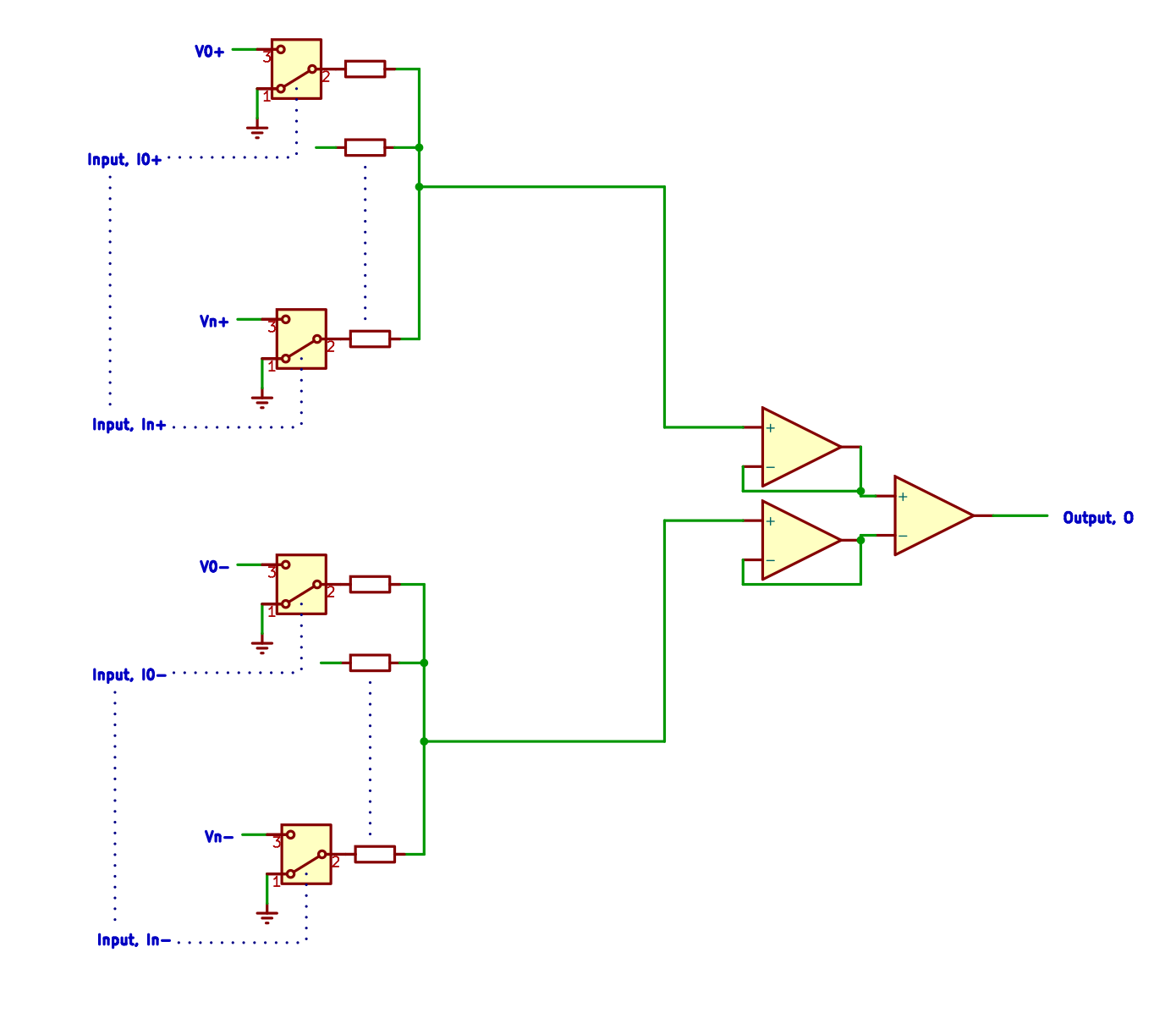 This is the central idea for a single artificial neuron. There are a number of digital inputs I0+…In+ and I0-…In+. Each controls an electronic analogue switch (SN74LVC1G3157) that selects either GROUND or a voltage, V. The voltages are set by digital to analogue converters (AD5629R) and are the weights in the network. There are exitatory inputs (I+) and inhibitory ones (I-). They are all summed by two operational amplifiers (MCP6004) the voltages from which are fed into a comparator to give the final output, O.
The neuron has fired when O = 1, and not when O = 0.
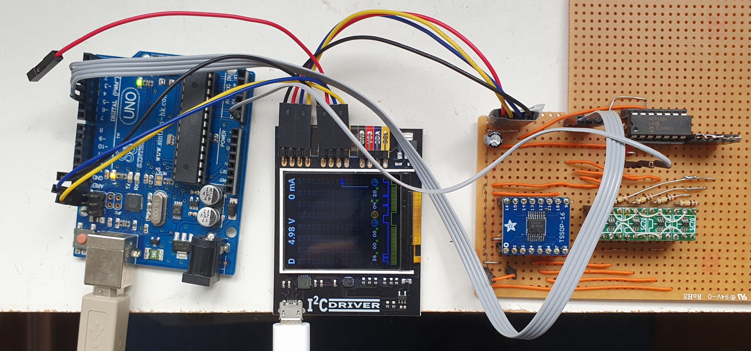
The photograph above shows a test breadboard of this design using the chips listed. The D to A converter and the Arduino are both controlled by the I2C driver in the middle, which allows the whole thing to be run via a single USB from a Python program running on a PC. The Arduino is supplying the inputs, I, and is reading and reporting the output voltage from the summing op. amp.
So far, so straightforward (I hope). It’s an analogue version of the way that a conventional artificial neural network operates, but it’s a lot closer to the biological original than linearising the thing in a program for a Turing-equivalent machine.
But I obviously don’t want to hard-wire the connections. I want the input data to be routed to any I input; I want the resulting weights/voltages to be routable in any combination to be summed; and I want any output, O, to be able to feed into any group of inputs, I, in the next layer (or to form a bit of the final result). To do this I will use crosspoint analogue switches (ADG2188).
First, here is how the voltages will be connected to the summing amplifiers:

Only one analogue switch in any row can be closed, but any number in a column can be closed. The closed switches in a column cause the corresponding voltages selected by the inputs, I, to be summed. This happens in adjacent pairs, one (left) inhibitory, and one (right) exitatory. The inputs on the left are labelled “synapses”, but it is perhaps more accurate to regard a single column of switches to be synapses.
So now there are a collection of outputs, O. These have to be connected to the inputs of the next layer, or form part of the final result:

The switch matrix works in exactly the same way as before (though there are different numbers of rows and columns), but this time it is switching digital signals. Once again only one switch on a row may be closed, but any number in a column may be closed. So any output, O, can be routed to any number of inputs, I, but each input can only be driven by one output.
There are also GROUND and Vdd columns that allow any input to be set permanently to 0 or 1. I may add a third such column carrying Johnson–Nyquist noise so that noise can be injected into the machine in a controlled way at any point.
If you look at the two diagrams above, you can see that they align, in the sense that they are two flat circuits that could be put one on top of the other then connected along their left and bottom edges.
Rather conveniently, the AD5629R D to A converter has eight analogue outputs, and the ADG2188 crosspoint switch is an 8×8 matrix. This will allow the whole system to be made modular – the synapses down the left in the first matrix diagram can be grouped in eights; the MCP6004 summing amplifiers along the bottom have 4 per chip and so can also easily be grouped in eights; and the matrix can be made up from 8×8 elements.
This means that the whole machine can be made Lego-like from just three modular PCB designs that can be combined with connectors for the edges to build a machine of any size. Of course there will be limits set by things such as input impedances, propagation delays and so on. Those will have to be calculated and experimentally investigated.
The whole machine will be programmed via I2C setting the voltages, V, and deciding which switches to close. Note that this will be done just once before the machine is used, and does not have to be altered while it is operating. Thus that step doesn’t have to be particularly fast. The voltages, and possibly the interconnections, will have to be altered when the machine is learning, though.
This means that there will be multiple identical I2C devices on the same bus, all with the same addresses. But these particular chips all have two addresses that you flip between with a 1 or a 0 on a given pin. So you can use that pin as a chip select – keep it normally 0, and just set it to 1 when you want to talk to the device on its 1-address.
But how to address all those address-select pins? Well. The computer can only talk to one device at a time; there is no parallelism while the machine is being set up, even though it is completely parallel in operation. And – as I pointed out above – for setting up the machine speed is not a big issue. So I propose that each I2C device will have a single D-type flip-flop (74LVC1G175GW) with its Q output connected to its address-select pin. These will be chained to make a long shift register. The controlling computer can reset all the flip-flops to 0 with a common CLR line then clock a single 1 into the first flip-flop to address the I2C chip on its Q output. The next clock pulse will allow the next device to be addressed, and so on.
What will the proposed machine be able to do? Well, as I mentioned I don’t yet know how big it can be made by adding more modules, though I’ll be very surprised if it can do a trillion-parameter LLM. It might make a component of one though. And it should be good for all sorts of pattern recognition tasks.
The machine is, provably, functionally complete because it can implement a NAND gate. (Functional completeness means that it can do anything that a computer can do.) To see this imagine that Vdd is used to switch 0.5V to the positive sum of one of the summing amps. Two of the I inputs then each switch 0.3V to the negative sum. Only when both inputs are 1 will the output be 0 – that is, that tiny bit of the machine becomes a NAND gate the output of which can be connected to any other input.
Unlike a conventional layered neural network (which the machine will also do), the machine can also implement feedback because outputs can be connected to inputs further back in any layers that are switch-connected together.
If it all works it will make a fully asynchronous (it has no clock in operation) modular neuromorphic analogue neural net. The entire design will be open-source, of course. And, if it works well, we may offer kits of the three basic modules plus edge connectors so that people can experiment.
All files and other details can be found in our Github repository here.
Adrian Bowyer
7 May 2024
Connect with us
Keep up to date on the latest RepRap Ltd news:
I would like to know, whether this has any advantages compared to a more traditional neural network in software format, if all the system are running perfectly.
The short answer is we won’t know until we build it. But it may well offer a lower power alternative, for example. Conventional software ANNs have been through a rather strange evolution: we took a massively parallel natural system and serialised it, taking advantage of the much faster speed of a von Neumann machine. But with big systems even that doesn’t scale, so we re-parallelized it using a piece of hardware that we happened to have lying around: graphics processors. Why not use a genuinely parallel architecture from the start, which is what this is?
A few weeks ago I read this and even now I’m no less impressed. Will you please let me mirror its Github at CodeBerg.org?
I’m offering to do it on your behalf because you’re surely busy. CodeBerg’s ethos more closely mirrors your own, the ethos behind this and RepRap both. That, and your idea is valuable: it hurts to imagine it being lost to time. (On a related note, this post is merely the highlight of a blog that already brings me a lot of joy and enrichment! I live in the United States. People here think science is wokeness and compassion is weakness, so when I’m reminded of people like you I’m reassured the insanity is localized to this piteous excuse for a country.)
Hi – yes, of course you can fork the repo and put it up at CodeBerg.org. Glad you find it interesting!
Best wishes
Adrian