Summary (TL;DR)
This describes a working design for an optical neural-net synapse that will use photons to transmit a weighted signal to a summing optoelectronic artificial neuron. We also have a design for the neuron itself, which we will build then describe in Part 2. In addition to working at the speed of light, another killer-app aspect of this is the number of input synapses you can have to one neuron, which turns out to be about the same as those to a human brain cell, and the number of outputs, which is similar.
The Idea
The problem with electronics is that electrons dawdle about. Light, on the other hand, works at – well – the speed of light.
So the idea here is to make a fast optical synapse for an artificial neural net, such as the one used for the GPT-3 AI, Google Translate, artificial face generation and all the other countless deep learning systems that are out there these days.
People have made optical neural networks using holograms before, but, once the hologram has been made, the network cannot be altered; it is taught, then it becomes fixed. What we wanted to do was to make a neural network that would operate at the speed of light, but that could also be taught and re-programmed indefinitely. And we wanted to take advantage of the fact that, while the in-use phase of a neural network needs to be as fast as possible (photons), we don’t much care if its learning phase is slow. In fact, we will be using chemistry for the learning phase, which is glacially slow compared to both electronics and photonics.
So what we need is two things: the first thing (one synapse) will use light to control the flow of more light, and the second will add and subtract the intensity of many streams of light from those synapses on dendrites to produce a single-axon light output – the equivalent of a neuron. We will need to use some electronics, particularly in the slow teaching phase, but as much as possible of the in-use phase will be done using light.
Let’s start with the synapse. It’s based on photochromism – the principle behind variable-darkness sunglasses. The idea of using photochromism for data storage was initially proposed by Yehuda Hirshberg in 1956.
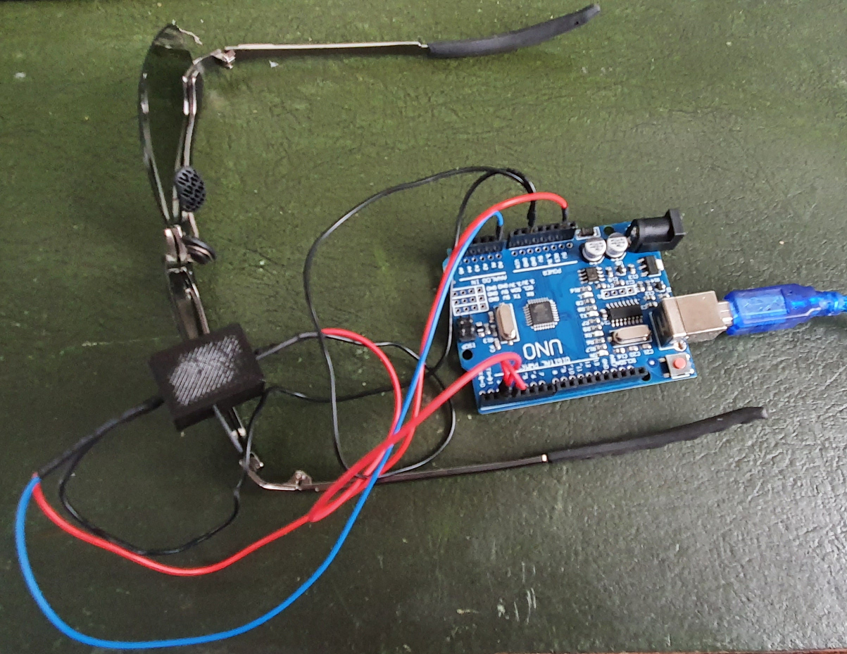
We made the prototype synapse with a pair of sunglasses from Ebay (£4.49…):
What’s going on here? Photochromism (at least in sunglasses) works using ultraviolet (UV) light. A transparent material – in this case the lenses of the glasses – is doped with a spiropyran or similar reversibly photochromic material. When UV light hits that, it becomes more opaque. When the light is turned off the reaction reverses and the material becomes transparent again. In fact the photochemical reaction is going both ways at once, so the degree of darkness of the material is at an equilibrium that depends on the amount of UV light hitting it.
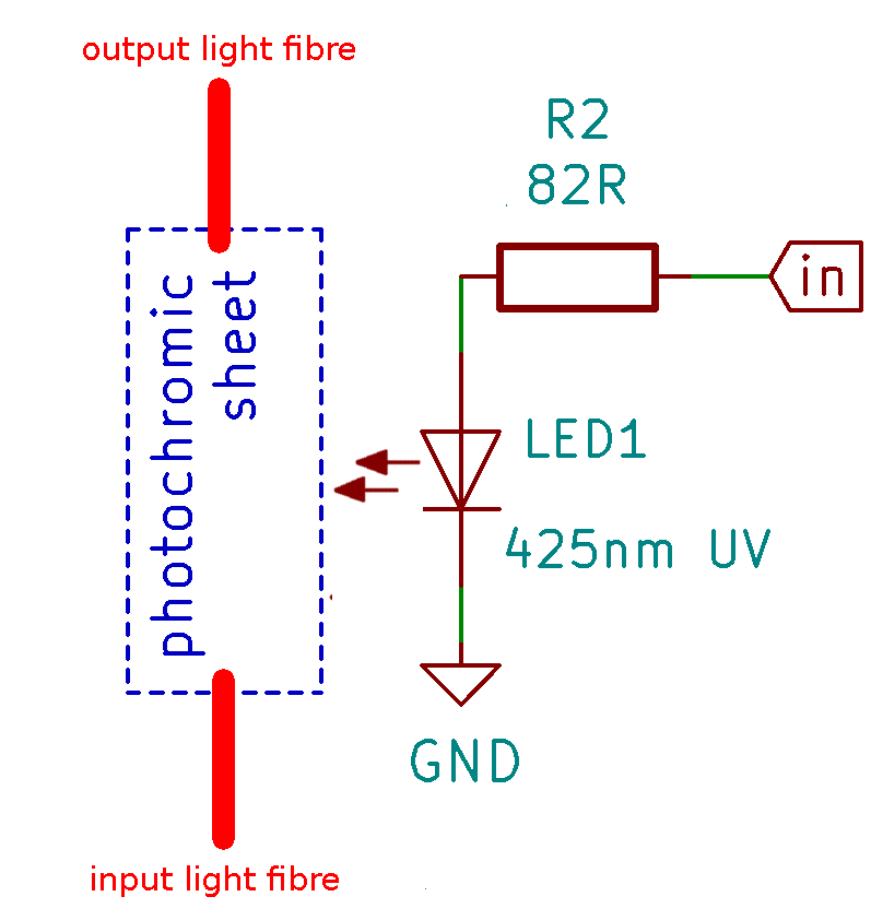
Here is a diagram of the device clipped over the lens above:
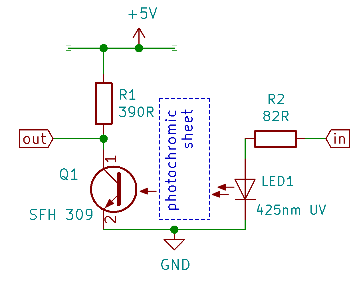
A UV LED is shining through the photochromic sheet onto a phototransistor. In the steady state this does not do anything very interesting: the sheet goes dark and the output voltage goes up as a consequence. It is a very slowly reacting signal buffer.
But if we drive the input with a pulse-width-modulated (PWM) signal, the photochromic sheet settles at a darkness decided by the mark-space ratio of the PWM. Its darkness remembers the magnitude of the PWM signal, and it can be read by looking at the output voltage when the UV LED is on. As you can see, it is hitched up to an Arduino UNO which we use to drive the UV LED and to monitor the voltage output.
So what we’ve done is to make an analogue optical memory. It needs to be refreshed (just as conventional RAM does) by the PWM signal, which is effectively writing to it, and it can be read very fast by pushing a full-brightness flash through it and reading the output voltage. The flash is so brief that it doesn’t darken the photochromic material.
(Technical note on the circuit diagram: from a quick experiment on collector current and gain, the collector resistor should ideally be 330Ω, but we didn’t have one…)
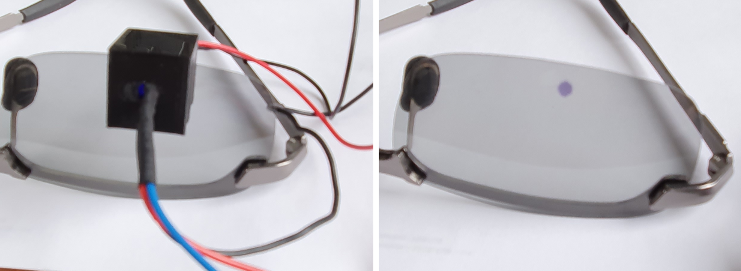
This is the first setup of the synapse, which has a body 3D-printed in black PLA. Here is a picture of it clipped to the sunglasses, and the resulting dark spot when it has been turned on at full UV LED power for about a minute:
Experimental Results
The first experiment we did was just to turn the UV LED on, monitor the output voltage until it stablised, and then turn it off and watch the decay in that voltage:
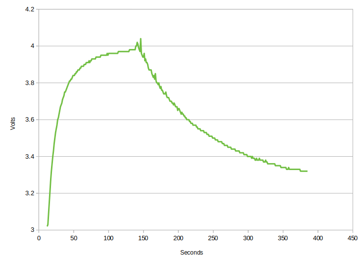
The device behaves very much as you’d expect. The photochromic lens takes about two minutes to stabilise as fully dark. When it recovers its transparency that takes rather longer.
Next we tried various PWM mark-space ratios. The Arduino uses 8 bits to define a PWM signal, so the range of average brightnesses goes from 0 to 255. Here is are the response curves to brightnesses of 0.25 (PWM = 63), 0.5, 0.75 and 1.0 of full brightness:
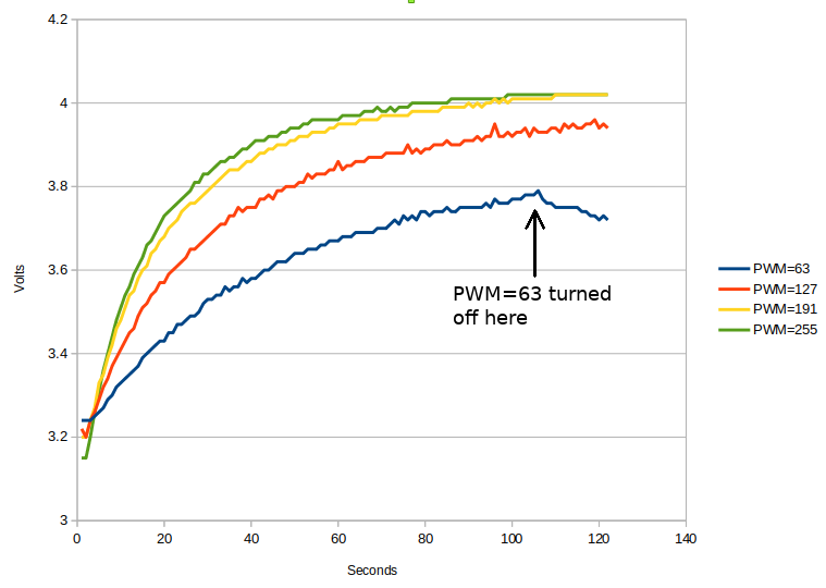
Again the synapse behaves as you’d expect: the brighter the average UV light level, the darker the photochromic material, and the lower the phototransistor collector current. So the voltage when it stabilises is higher. (The PWM=63 experiment was turned off early by mistake…)
The particular photochromic material in the Ebay sunglasses seems to saturate at about 0.8 of full UV LED intensity, so that puts a restriction on the range of PWM values that can usefully be used, but that shouldn’t be any problem in practice. And there is clearly a lot of room for messing about between 0 and 63.
From Synapse to Neuron
We don’t have to configure the final synapse design in quite that way instantiated above. Instead we would do this:
Now we have a refreshed memory device that is being written electronically by the PWM signal, but that can be read by the light passing through from the input light fibre to the output. Note that we don’t have to use the same reading wavelength as the writing one; in particular we could choose a long wavelength that had no effect on the photochromic material if we wanted to.
So how do we make the neuron to which this would be just one of (possibly thousands) of inputs? We simply bundle the output light fibres from many synapses together and point them at a single phototransistor. This will have the effect of adding all the light up without the need for complicated circuitry – the output of the phototransistor would depend on the sum of all the light going into it.
Now, we need both inhibitory and exitatory inputs. To achieve this we optically split each input fibre in two and run each through their own adjustable photochromic synapse. Then, when they all come together as the summing input, we route one of each pair to one phototransistor, and the other to a second phototransistor. We arrange those phototransistors as a long-tailed pair to subtract one set of inputs from the other.
Obviously we are doing all this with big clunky components that are easy to handle and to experiment with. But it should be straightforward to miniaturise everything and to make and optically and electrically to interconnect tens of thousands of these devices on a single chip using standard IC fabrication lithography.
In addition to working at the speed of light, another real killer-app aspect of this is the number of input synapses you can have to one neuron, which turns out to be about the same as those to a human brain cell, and the number of outputs, which is similar. More details of, and experiments on, the neuron when we’ve made it in the next post: Part 2…
Downloads
For all the files for this project (which, at the moment, is very much incomplete) see Github here.
The Next Step
The next post on this project is here.
Connect with us
Keep up to date on the latest RepRap Ltd news: